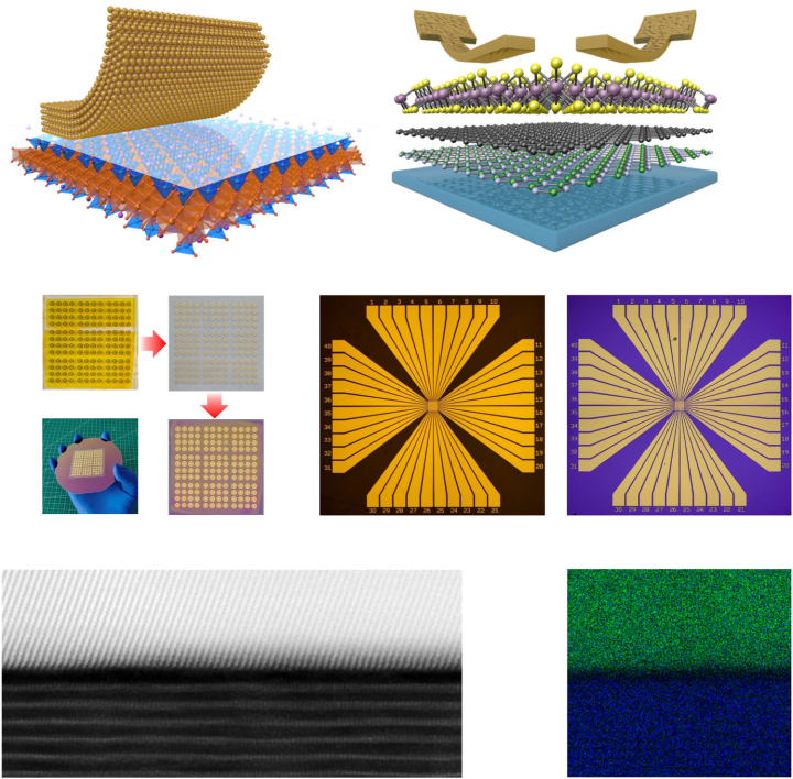
A research team led by ICQD members, Prof. ZENG Hualing and Prof. QIAO Zhenhua, along with Prof. SHAO Xiang from the University of Science and Technology of China (USTC) of the Chinese Academy of Sciences (CAS) achieved progress in studying van der Waals (vdW) contacts for two-dimensional (2D) electrical devices. The team developed an innovative all-stacking technique for fabricating 2D electrical devices, optimizing the interface contact between 2D materials and metal electrodes. The study was published online in Nature Communications.
In conventional fabrication processes for 2D electrical devices, the deposition of metal electrodes is a critical step. High-energy metal atoms deposited on the surface of 2D materials can easily damage their lattices, ultimately degrading the device's electrical performance. Therefore, achieving reliable electrical contact between 2D materials and metal electrodes is crucial for improving the performance of 2D electrical devices.
Recent research has shown that for 2D electronic devices, realizing the vdW contact holds promise for solving the above problems. The vdW contact refers to the interaction between 2D materials and metal electrodes through vdW forces. This method avoids introducing numerous defects and can achieve good electrical contact, offering better operability and potential for large-scale application.
To achieve reliable 2D vdW contacts, the team developed an all-stacking technique. This technique allowed for the direct stacking of metal electrodes onto 2D materials during the fabrication of 2D electrical devices, avoiding steps like metal deposition and thus protecting the 2D materials from damage while achieving excellent electrical performance.
Specifically, 2D electrical devices fabricated using this technique had sharp metal-semiconductor contact interfaces, with smooth and clear vdW gaps at the interface and no metal atom doping on the 2D material side. This indicated that high-quality vdW contact had been formed between the metal electrodes and the 2D semiconductor.
Due to the improved contact interface, 2D semiconductor transistors fabricated using this technique exhibited more than 95% reduction in off-state current and a 50% decrease in subthreshold swing compared to those fabricated using metal deposition processes. They also possessed a higher on-off ratio, making them more advantageous for low-power integrated circuits.

Illustration of electrode transfer and the all-stacking method. (Image by USTC)
To demonstrate the potential of the all-stacking technique for wafer-scale manufacturing, the team fabricated an array of field-effect transistors based on monolayer molybdenum disulfide using this technique. The device yield was as high as 98.4%, exhibiting excellent consistency and stability. The average on-off ratio of the transistor array was 6.8×10⁶, with 91.3% of the devices having an on-off ratio greater than 10⁶. The excellent performance and high consistency of the transistor array demonstrated the advantages of the all-stacking technique in achieving reliable contact for 2D electronic devices.
The all-stacking technique developed in this study optimizes the interfacial contact between 2D materials and metal electrodes, providing an efficient, high-quality, and universal approach for the preparation of 2D electronic devices. The study is expected to provide a new technical path for the industrial-level manufacturing of future 2D electronic devices.
Paper link: https://www.nature.com/articles/s41467-024-49058-7
